![[Ready To Publish] AI Is Changing Which Semiconductor Capabilities Matter_Lucy Jenyi Chang_Image](https://heckelai.com/wp-content/uploads/2026/09/Ready-To-Publish-AI-Is-Changing-Which-Semiconductor-Capabilities-Matter_Lucy-Jenyi-Chang_Image.png)
The $3.5 Billion Question
A smartphone chip and a hyperscale AI accelerator appear to belong to opposite ends of computing. One is shaped by battery life, tight thermal limits and enormous production volumes; the other by high-bandwidth memory, advanced packaging and data centres constrained by power and data movement at massive scale. Yet on August 31, NVIDIA invested $3.5 billion in convertible bonds issued by MediaTek while expanding their collaboration across AI infrastructure, local AI computing and automotive. MediaTek will also adopt NVIDIA’s NVLink Fusion platform to help customers develop custom AI processors for rack-scale systems.¹
The investment does not prove that MediaTek will become a leading AI-chip supplier, but it makes the company’s unusual competitive path into AI infrastructure hard to ignore and worth examining. Why are capabilities accumulated by a company still widely associated with smartphones becoming strategically relevant to hyperscale AI?
When The Constraints Change, So Does Capability Value
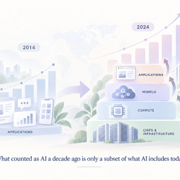
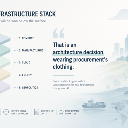
Part of the answer lies in what increasingly constrains AI performance. Raw compute remains essential, but power and data movement are becoming harder limits on how far AI systems can scale. SEMI describes AI competition as shifting from individual chips towards system-level integration, requiring compute, memory and interconnect to be increasingly co-designed.² TSMC has made a similar argument from another direction: surging electricity demand from AI is making energy efficiency, rather than computing power alone, a central constraint on future chip development.³ Manufacturability is becoming another constraint.⁴ As AI systems integrate more memory, chiplets and advanced packaging, tighter requirements for process control, uniformity and yield make those increasingly complex designs harder to manufacture reliably at scale.⁵⁶
A semiconductor capability does not gain value simply because it is sophisticated. Its strategic value rises when the problem it solves becomes more consequential. If AI changes the physical constraints that are hardest to overcome, it can also change the value of capabilities semiconductor companies accumulated long before the current AI boom.
A Different Path Into AI Infrastructure
That is what makes MediaTek a revealing comparison with established custom-silicon players. Broadcom entered the AI era with more than three decades of complex ASIC experience rooted in wired communications and applications including high-speed computing, networking and storage.⁷ Marvell followed a different path, but spent the past decade deliberately transforming itself around data infrastructure, adding custom ASIC, compute and high-speed connectivity capabilities through acquisitions and portfolio changes.⁸ Their routes into AI infrastructure are easier to trace because much of their capability base was already shaped around infrastructure problems.
MediaTek’s historical path is different. The company says it uses the high volume and scale of its mobile business to optimise yield and process technology, then applies those learnings to large-scale data-centre designs. It also explicitly links its experience with low-voltage mobile operation to data-centre compute efficiency.⁹ Semiconductor research provides a broader reason to take accumulated experience seriously: organisational routines and learning around new semiconductor process technologies can contribute to enduring differences in manufacturing performance.¹⁰
Smartphone technology cannot simply be transplanted into an AI accelerator. What may carry across markets is the know-how accumulated by repeatedly bringing leading-edge silicon into high-volume products while managing difficult trade-offs among power, process technology, integration and manufacturability. AI data centres remain a radically different engineering environment. But as power and manufacturability become harder constraints on AI scaling, some of the underlying disciplines shaped by mobile become more strategically relevant. AI did not make smartphones and data centres technologically similar. It made some of the constraints that shaped mobile semiconductor capabilities relevant at hyperscale.
Relevance Is Not Sufficiency
Becoming more relevant to AI is not the same as being fully equipped for it. If MediaTek’s mobile experience were sufficient by itself, the company would not need to build the infrastructure-specific capabilities that hyperscale AI demands. MediaTek now highlights high-speed SerDes, HBM integration, advanced packaging and rack-level integration as parts of its data-centre offering.⁹
Independent reporting also shows that it is still strengthening its advanced-packaging capabilities, including recruiting experienced talent from TSMC.¹¹
What is happening at MediaTek is not a straightforward transfer of mobile capabilities. It is a recombination, pairing experience developed through mobile with technologies and system expertise built specifically for AI infrastructure.
AI can increase the relevance of capabilities accumulated in an earlier computing market without making those capabilities sufficient for the new one. Turning that relevance into competitive position still requires complementary technologies, system expertise and execution at an entirely different scale. In this context, NVIDIA’s investment matters because it signals that MediaTek’s transition has become strategically consequential. The investment alone does not show that the transition is complete. NVIDIA itself describes bringing custom accelerators into production as requiring integration across multi-die architectures, advanced packaging, high-speed SerDes, HBM, I/O and scale-up networking.¹
AI Is Changing The Competitive Map
MediaTek’s case points to a broader shift in semiconductor competition. Semiconductors are where AI’s ambitions ultimately encounter physical limits. Software can demand ever more scale, but the infrastructure beneath it must still move data, manage power and heat, integrate memory and turn increasingly complex designs into manufacturable systems. As those limits change, the semiconductor capabilities that carry strategic value can change with them.
Broadcom and Marvell retain deep infrastructure advantages, and mobile expertise does not automatically translate into hyperscale success. But MediaTek suggests that the next generation of credible AI-infrastructure competitors may not be fully predictable from historical market labels. As AI pushes computing against new physical limits, the semiconductor race may increasingly reward not only companies that built for the data centre first, but those whose accumulated capabilities best fit the constraints AI creates next.
References
¹ NVIDIA Corporation (2026), NVIDIA and MediaTek Deepen Long-Standing Partnership to Build AI Edge to Cloud Computing Platforms. NVIDIA Newsroom, 31 August. Available at: https://nvidianews.nvidia.com/news/nvidia-and-mediatek-deepen-long-standing-partnership-to-build-ai-edge-to-cloud-computing-platforms (Accessed: 7 September 2026).
² SEMI (2026), AI Power Constraints Drive System-Level Integration: SEMICON Taiwan 2026 Spotlights Breakthroughs in Design, Memory, and Optical Interconnect, 6 August. Available at: https://www.semi.org/en/node/174306 (Accessed: 7 September 2026).
³ Sterling, T. (2026), ‘Energy use forcing rethink of AI chip design, TSMC says’, Reuters, 28 May. Available at: https://www.reuters.com/business/retail-consumer/energy-use-forcing-rethink-ai-chip-design-tsmc-says-2026-05-28/ (Accessed: 7 September 2026).
⁴ Haley, G. (2026), ‘Advanced Packaging Limits Come Into Focus’, Semiconductor Engineering, 19 March. Available at: https://semiengineering.com/advanced-packaging-limits-come-into-focus/ (Accessed: 8 September 2026).
⁵ Applied Materials (2026), DRAM and Advanced Packaging Define the Future of Energy-Efficient AI, 22 June. Available at: https://www.appliedmaterials.com/us/en/newsroom/blogs/dram-and-adv-packaging-define-the-future-of-energy-efficient-ai.html (Accessed: 8 September 2026).
⁶ An, J. and Zhao, K. (2026), ‘Tackling Key HBM and Advanced Packaging Bottlenecks for the AI Era’, Applied Materials, 18 August. Available at: https://www.appliedmaterials.com/us/en/newsroom/blogs/tackling-key-hbm-and-advanced-packaging-bottlenecks-for-ai-era.html (Accessed: 8 September 2026).
⁷ Broadcom Inc., Application-specific Integrated Circuits (ASICs). Available at: https://www.broadcom.com/products/custom-silicon/asics (Accessed: 7 September 2026).
⁸ Marvell Technology, Inc. (2026), 2026 Proxy Statement. Available at: https://investor.marvell.com/sec-filings/all-sec-filings/content/0001104659-26-060253/tm261486-1_def14a.htm (Accessed: 7 September 2026).
⁹ MediaTek Inc., Data Center Solutions: Beyond the XPU: Innovating the Fabric of AI Scaling. Available at: https://www.mediatek.com/products/data-center (Accessed: 7 September 2026).
¹⁰ Macher, J. T. and Mowery, D. C. (2009), ‘Measuring Dynamic Capabilities: Practices and Performance in Semiconductor Manufacturing’, British Journal of Management, 20(s1), pp. S41–S62, 19 February. Available at: https://onlinelibrary.wiley.com/doi/10.1111/j.1467-8551.2008.00612.x (Accessed: 7 September 2026).
¹¹ TrendForce News (2026), ‘[News] MediaTek Ramps Up Advanced Packaging Push as TSMC Veteran Shang Hou Calls for More Talent’, 1 September. Available at: https://www.trendforce.com/news/2026/09/01/news-mediatek-ramps-up-advanced-packaging-push-as-tsmc-veteran-shang-hou-calls-for-more-talent/ (Accessed: 7 September 2026).